

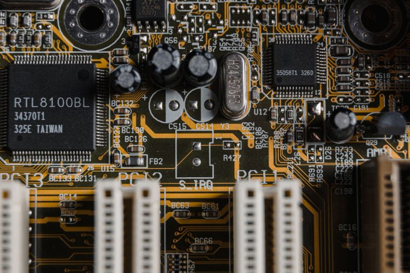
The Union Cabinet approved Semicon Mission 2.0 worth ₹1.27 lakh crore on July 15, 2026, extending India’s flagship semiconductor push to build a fuller domestic chip ecosystem. The Cabinet Committee on Economic Affairs (CCEA), chaired by Prime Minister Narendra Modi, cleared the scheme to widen incentive support beyond fabrication plants into packaging, testing, and specialty chip segments.
Semicon Mission 2.0 builds on the original India Semiconductor Mission launched in 2021 and is administered by the Ministry of Electronics and Information Technology (MeitY). The new outlay nearly doubles the government’s earlier commitment and is aimed at attracting global chipmakers while reducing India’s dependence on imported semiconductors for electronics, automotive, telecom, and defence manufacturing.
How Will Semicon Mission 2.0 Affect Indian Manufacturers?
The scheme extends fiscal support to compound semiconductors, silicon photonics, sensor fabrication, and chip packaging units — segments largely excluded from the first mission. Electronics manufacturers and automotive component makers are expected to benefit from shorter supply chains and lower import costs, as the mission targets a domestic value-addition push across the ₹1.27 lakh crore outlay. Officials indicate the scheme will also fund advanced packaging (ATMP/OSAT) facilities, which create more jobs per unit of investment than wafer fabs.
What Do Industry Bodies Say?
Industry groups including the India Electronics and Semiconductor Association (IESA) have welcomed the expanded scope, noting that packaging and testing capacity has lagged behind fab investment under the first mission. Analysts tracking the sector say the CCEA’s decision signals continuity of policy support beyond the initial four-year window, which is critical for global semiconductor firms evaluating multi-year capital commitments in India.
Market and Trade Reaction
Shares of domestic electronics manufacturing services (EMS) and semiconductor ancillary companies saw active trading interest following the announcement. The move also comes as India seeks to position itself as an alternative node in global semiconductor supply chains amid continuing US-China tech tensions and export control regimes on advanced chips.
What Happens Next?
MeitY is expected to notify detailed scheme guidelines and application windows for Semicon Mission 2.0 in the coming weeks. Industry watchers will track how many new fab, ATMP/OSAT, and compound semiconductor proposals are approved under the scheme, and whether large global players commit fresh investment following the CCEA clearance.
Frequently Asked Questions
What is Semicon Mission 2.0?
Semicon Mission 2.0 is the Indian government’s expanded ₹1.27 lakh crore scheme, approved by the Cabinet on July 15, 2026, to support semiconductor fabrication, packaging, testing, and compound chip manufacturing across India.
How much funding was approved for Semicon Mission 2.0?
The Cabinet Committee on Economic Affairs approved a total outlay of ₹1.27 lakh crore for the mission’s second phase.
Which ministry oversees Semicon Mission 2.0?
The Ministry of Electronics and Information Technology (MeitY) administers the scheme and will issue detailed implementation guidelines.











Leave a comment