

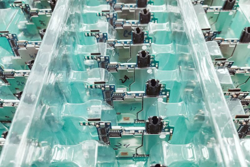
Prime Minister Narendra Modi inaugurated SEMICON India 2026 at Yashobhoomi in New Delhi on September 17, launching Semicon 2.0, a ₹1,27,500 crore ($13.5 billion) second phase of India’s semiconductor mission that extends state support beyond chip fabrication plants to equipment, materials, design, research and talent development. The move signals New Delhi’s intent to build a complete, self-reliant semiconductor value chain rather than just assembly capacity.
The Union Cabinet approved Semicon 2.0 in July 2026, and its formal unveiling came as SEMICON India 2026 drew more than 600 participating companies, 52 countries and roughly 50,000 visitors under the theme “Sand to Silicon to Systems.” The scheme builds on Semicon 1.0, under which three of the 12 approved projects have already begun commercial production, giving the government evidence that its subsidy-driven model can deliver working fabs rather than announcements alone.
What Does Semicon 2.0 Cover Beyond Chip Fabs?
Semicon 2.0 is structured around six pillars that widen incentives from fabrication and packaging to upstream and downstream segments: semiconductor equipment manufacturing, specialty materials and chemicals, chip design and intellectual property, applied research, workforce and talent development, and systems integration. Officials say this broader scope is meant to fix a gap in Semicon 1.0, where India attracted fab and packaging investment but remained dependent on imported equipment and materials, leaving the ecosystem vulnerable to supply disruptions.
How Will Manufacturers and Investors Be Affected?
Companies across the semiconductor supply chain, from equipment makers to fabless design startups, become eligible for capital support and production-linked incentives that were previously concentrated on large fab operators. For electronics and industrial manufacturers who depend on chip supply, the pledge of a more complete domestic ecosystem is aimed at reducing lead times and foreign-exchange exposure on components, a recurring pain point since the 2021 global chip shortage. Global equipment and materials suppliers now have a clearer incentive structure to set up Indian operations rather than serve the market purely through exports.
What Do Industry Bodies and Analysts Say?
Industry body SEMI, which co-organizes the event, framed Semicon 2.0 as validation that India’s semiconductor programme has moved from policy intent to industrial execution, pointing to the commissioning of Semicon 1.0 projects as proof of delivery. Analysts tracking the sector note that India’s approach mirrors moves by the United States, the European Union and Japan to de-risk semiconductor supply chains through direct subsidies, positioning India to compete for a share of chip investment that manufacturers are diversifying away from a China-concentrated base.
Market and Trade Reaction
Shares of listed electronics manufacturing and components companies saw increased trading interest around the SEMICON India 2026 dates, with investors positioning for downstream beneficiaries of expanded state support. Trade watchers noted that a stronger domestic materials and equipment base could, over time, reduce India’s import bill for semiconductor manufacturing inputs, a category that has grown alongside the ramp-up of Semicon 1.0 fabs in Gujarat and Assam.
What Happens Next?
The government is expected to open the formal application window for Semicon 2.0 incentives in the coming months, with the Ministry of Electronics and Information Technology (MeitY) likely to issue detailed scheme guidelines covering eligibility, subsidy caps and timelines for each of the six pillars. Industry watchers will track how many equipment and materials firms commit to Indian investment in the next two quarters as the clearest early signal of the scheme’s traction.
Frequently Asked Questions
What is Semicon 2.0?
Semicon 2.0 is the second phase of India’s semiconductor mission, approved by the Union Cabinet in July 2026 with an outlay of ₹1,27,500 crore. It extends incentives from chip fabrication and packaging to equipment, materials, design, research and talent.
How is Semicon 2.0 different from Semicon 1.0?
Semicon 1.0 focused mainly on attracting fabrication and packaging plants, three of which have started commercial production. Semicon 2.0 widens support to the full value chain, including equipment makers, materials suppliers, chip designers and research institutions.
Who benefits from Semicon 2.0 incentives?
Semiconductor equipment manufacturers, specialty chemical and materials suppliers, fabless chip design firms, research institutions and systems integrators are all eligible, in addition to the fab and packaging companies supported under the earlier scheme.











Leave a comment